128 Series
Silicon Concepts is the leading manufacturer of stress measurement tools for semiconductor, MEMS, optoelectronic, and flat panel applications. Stress and wafer bow maps can be acquired over the entire wafer surface, providing process engineers means to characterize and develop new processes using different thin film materials.
The SIC 128 Series systems are room temperature, full-wafer 2D/3D stress mapping systems. 128 systems use SIC's patented non-contact Opti-Lever dual-laser auto-switching technology. Ability to scan 1000 points per inch in seconds for high resolution, high precision stress mapping on blanked and patterned wafers.
128L C2C
Dedicated Film Stress mapping system with high resolution for high throughput process control. Fully automated cassette to cassette, SECS/GEM compliant 300mm Film Stress and Bow Measurement tool. Dual or single FOUP configurations available. Integrated wafer substrate thickness measurement available.
128L
Film stress and wafer bow measurement for wafers up to 300mm wafer. 2D/3D stress mapping standard. Semi-automated system with convenient wafer loading and retrieval.
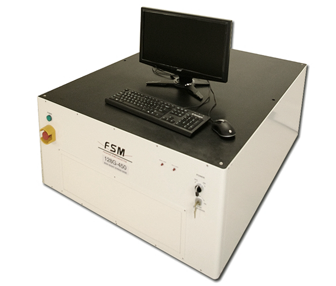
128G-450
Film stress and wafer bow measurement for wafers up to 450mm wafer or flat panel displays. 2D/3D stress mapping standard. Semi-automated system with convenient wafer loading and retrieval.
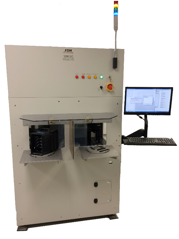
128 C2C
Dedicated Film Stress mapping system with high resolution for high throughput process control for wafers up to 200mm diameter. Fully automated cassette to cassette, SECS/GEM Film Stress and Bow Measurement tool. Dual or single load port configurations available. Integrated wafer substrate thickness measurement available.
413 Series
Substrate and tape total and individual thicknesses, warpage, and TTV Measurement. Able to measure with or without backing tape. For wafer back-grind and etch thinning processes control. Non-contact Echoprobe or VITE Technology. Thin film and surface roughness options.
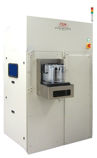
413 C2C
Thickness and total thickness variation (TTV) mapping system. TTV and Thickness of wafer substrate, thick layers, wafers on tape, bonded wafers, etc. Fully automated cassette to cassette system, SECS/GEM compliant. Warp, Roughness, and Thin Film Thickness measurement options.
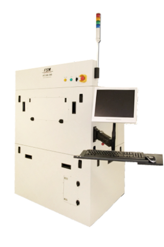
413 SA
Thickness and total thickness variation (TTV) mapping system. TTV and Thickness of wafer substrate, thick layers, wafers on tape, bonded wafers, etc. Semi-automatic system with enclosure. Manual loading, automatic measurement. Warp, Roughness, and Thin Film Thickness measurement options. Systems up to 300mm diameter wafers with or without frame.

413 PR
413PR is specially designed for automatic substrate thickness measurement on wafers with optically turbid (milky) tapes, as well as for applications demanding fast, reliable, automatic measurement site location. Special optics and illumiation allow rapid location of areas of interest. Semi-automatic system with enclosure for wafers up to 300mm with or without frame..

413MOT
Thickness and total thickness variation (TTV) mapping system. TTV and Thickness of wafer substrate, thick layers, wafers on tape, bonded wafers, etc. Manual loading, auto-mapping. Warp, Roughness, and Thin Film Thickness measurement options. Systems up to 300mm diameter wafers with or without frame.
500 Series
Stress Hysteresis Measurement up to 500C for thermal property and stability tests of thin films in inert gas. Non-Contact Laser Scanning Technology.
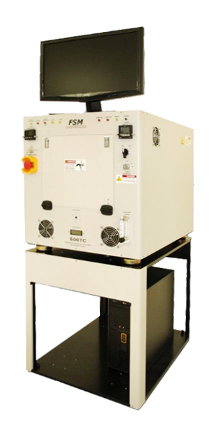
500TC
Evaluate the thermal properties and stability (film stress) of thin films up to 500 degree C in inert gas. 200mm or 300mm chamber. Manually loading.
900 Series
Stress Hysteresis in vacuum or gas up to 900C for the study of annealing cycles. Thermal Desorption, Film Shrinkage, Reflectivity, and Resistivity options provide additional insight to causes of material changes with temperature. NEW: Optional wafer rotation offers unique 2D/3D mapping to study wafer deformation as a function of temperature.
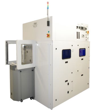
900 C2C
Rapid Thermal Mechanical Characterization of novel materials. Simulataneous extraction of stress hysteresis, thermal desorption, film shrinkage and reflectivity data during thermal cycling in vaccum up to 900 degree C. Fully automated cassette to cassette system for 300mm wafers. SECS/GEM option.
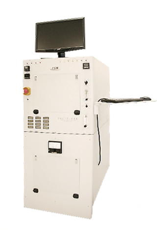
900TC-VAC
Rapid Thermal Mechanical Characterization of novel materials. Simulataneous extraction of stress hysteresis, thermal desorption, film shrinkage and reflectivity data during thermal cycling in vacuum up to 900 degree C. Manually loading system.
Adhesion Testers
Film adhesion testing of thin films and stacks on substrates for material evaluation.
MELT
Modified Edge Liftoff Test to measure adhesion of thin film and thin film stacks on a wide variety of crystalline and non-crystaline substrates, such as Silicon, III-V compounds, glass, etc. Suitable for mid adhesion samples.
Aquaflex
4-Point Bend film adhesion test. Measurement in air or liquid. For low to mid adhesion samples. Multi-chamber option for rapid testing.
Electrical Characterization
Contact and Non-Contact sheet resistance measurement systems for implantation, diffusion, metallization, and many other applications.
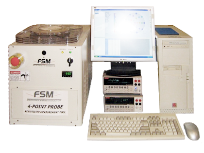
4pp
4-Point Probe Technique for measuring the sheet resistance of epi, metal films, substrates. Table top and fully automated cassette to cassette systems available.
Raman 360 and FSM127
Local and Lattice Stress Measurement, Die level Topography. For in-die and in-device stress and composition control.
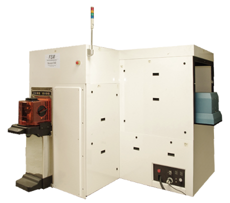
Raman-360
Micro Raman system for lattice level strain and material composition measurement. High spectral resolution (0.02 cm-1) and sub micron lateral resolution. Measurement of through silicon via (TSV) keep out zone, local stress and composition profiling. Fully automated C2C system.
VIT(E) Series
Virtual Interface Technology for 3D-IC Metrology: TSV profile (depth, top & bottom CD) , Remaining Silicon Thickness (RST), Copper Nail Height, Bump Height and Cu pillar Height, Edge trim profile.
VIT C2C
Dimensional metrology system for 3D-IC application: Through Silicon Via (TSV) depth, top CD, bottom CD, remaining silicon thickness (RST), copper pillar height, bump height, and many more. Fully automated cassette to cassette system for 300mm wafers. SECS/GEM option. Warp, Roughness, and Thin Film Thickness measurement options.
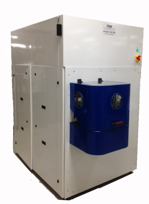
8108 VITE
New high speed, high accuracy non-contact characterization of thin wafers, through silicon vias (TSV), bumps, MEMS structures and novel materials. SIC 8108 VITE can be employed in the front-end and backend. It provides thickness, TTV, and topography of Si and compound materials, edge trim geometry, multilayer thickness and topography of wafers on tape, on sapphie,or on glass. Measurement of warp of highly warped wafers and measurement of thick films.
